

The Wonders of Electromagnetism
vol.3 Chip Type Components and the Internal Spiral Concept
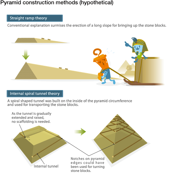
"Internal spiral shaped tunnel" theory may shed light on the mystery of how the pyramids were built
The pyramids in Egypt are one of the seven wonders of the ancient world. In particular, the Great Pyramid of Giza (also known as the Pyramid of Khufu) stands out as the most monumental stone building on earth, with a height of 147 meters and consisting of some 3 million limestone blocks averaging 2.5 tons in weight. Built in an age where no heavy construction machinery existed, many theories have been proposed as to how the pyramid was erected with human power alone. The most well known of these is the straight ramp theory, whereby a long slope was supposed to have been built, for dragging up the stone blocks using rope. Because such a slope would have to be extremely long, doubts were cast on this theory, but no better alternative explanation existed for a long time. However, in recent years a French architect advanced the so-called spiral tunnel theory, which has garnered considerable attention worldwide.
According to this explanation, a slope was built to about one third the height of the pyramid, and then a series of spiral shaped tunnels running just inside the outer walls was used for further transporting the stones. The internal tunnels eliminate the need for scaffolding, and a gently rising slope could be achieved through the spiral-shaped arrangement. Notches found at various locations on the pyramid's edges could be remnants of locations where the stone blocks were turned into a different direction. If this theory holds true, we can only marvel at the ingenuity of the Egyptian pyramid builders 5,000 years ago.
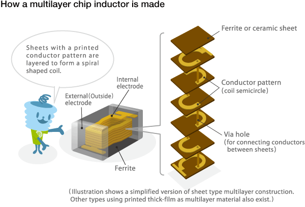
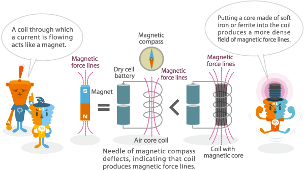
In 1980, TDK introduced the world's first multilayer chip inductor which was born out of an idea rivaling the pyramid construction method in brilliance. A typical example of multilayer construction in electronic components is the multilayer ceramic capacitor. Sandwiching dielectric layers with electrode layers is an approach that intuitively makes sense, but when it comes to inductors, forming a three-dimensional coil within the restricted thickness of a multilayer component does not seem feasible. But TDK successfully established a new technology for creating a coil by stacking layers, each containing a semicircle shaped printed conductor, thereby forming a kind of spiral stairway within the component. Along with multilayer ceramic chip capacitors, multilayer chip inductors came to play a vital role in making electronic devices smaller, thinner, and lighter.
LTCC method pushes the boundary of multilayering technology to integrate multiple passive components
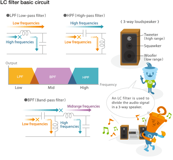
Inductors (coils) are characterized by the fact they will smoothly pass DC current but present a barrier to AC current. Interestingly, the higher the frequency of the AC current, the more it will be blocked by an inductor. By contrast, a capacitor will pass the higher frequency current more easily. The combination of an inductor (L) and capacitor (C) results in an LC filter, a component making use of these opposing properties. Depending on which frequencies are being let through, LC filters can be categorized into three types. A low-pass filter (LPF) only allows current beneath a certain frequency to pass. A high-pass filter (HPF) does the opposite, passing only current above a certain frequency. Finally, a band-pass filter (BPF) only passes current of a given frequency band between two cutoff points.
High-quality audio systems often use three-way speakers where the audible range is reproduced by three different types of drivers. LC filters present a convenient way to achieve this. The woofer handling the low end of the spectrum is driven via a low-pass filter, and the tweeter via a high-pass filter. A band-pass filter serves to provide the signal for the midrange driver.
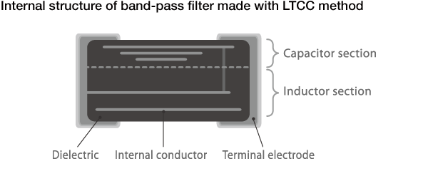
Band-pass filters are also a major component of the high frequency circuitry in mobile phones. Driven by the trend towards multi-band and multi-mode capability that allows a single phone to support various frequency bands and communication methods, the use of band-pass filters has risen dramatically. Computers and game consoles with Bluetooth and wireless LAN capability further contribute to this increase in demand. In keeping with the move towards multi-function support and high performance, band-pass filters also need to become ever smaller and lighter. As a way to achieve this, a technique called LTCC (Low Temperature Co-fired Ceramics) has been developed by further refining multilayering technology. The process involves an alumina-based glass ceramics substrate in sheet form. Multilayering is then used to form multiple passive components such as capacitors and inductors on the substrate. Compared to existing LC filters with discrete components, the new technique results in drastically reduced dimensions.
Thin-film electronic components realized with HDD head manufacturing technology
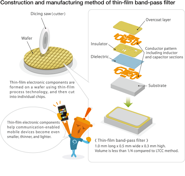
Chip components found on the high frequency circuit PCBs of a mobile phone are generally of the 0603 size (0.6 mm long x 0.3 mm wide x 0.3 mm high), which is smaller than a strawberry seed. Since the space available for the printed circuit board is extremely limited, the height of band-pass filters ideally should also be kept to a maximum of 0.3 mm. However, even with the LTCC method making optimum use of multilayering technology, there are limits as to how thin a component can be made.
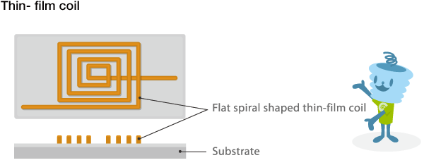
TDK therefore developed a thin-film process derived from HDD head manufacturing technology, achieving another breakthrough in terms of reduced footprint and component height. Photolithography, plating technology, vapor deposition, and other advanced processes are employed to form thin-film circuit components on the substrate. The first product realized by TDK with this method was a common mode filter featuring a combination of two coils for effective noise control. Thin-film process technology is used to create flat spiral-shaped thin-film inductors on the substrate.
Following the successful realization of the thin-film common mode filter, TDK next tackled the development of a thin-film band-pass filter. A number of difficult technical challenges had to be overcome while working on this project. Since a band-pass filter combines inductor and capacitor elements, the dielectric of the capacitor element has to be made very thin. Unlike multilayer ceramic chip capacitors that use a thick-film process, a thin-film capacitor must be fortified against electrostatic discharge, humidity and other factors, in order to achieve high reliability.
By applying highly stable process technology to the formation of the dielectric film, redesigning the electrode forming process, and modifying the connection method of terminal electrode and internal pattern, TDK was finally able to create a thin-film band-pass filter featuring the same high reliability as existing products. Designers of mobile devices with communication capabilities are always aiming for smaller dimensions, lower profile, and higher functionality. TDK is meeting demand in this area by expanding its lineup of thin-film high-frequency components, including thin-film baluns, thin-film couplers, and "Z-match" impedance matching thin-film capacitors.
TDK is a comprehensive electronic components manufacturer leading the world in magnetic technology
About TDK
Share Share this article
RecommendedPeople who viewed this article also viewed here
The Wonders of Electromagnetism
vol.4 Shrinking Size of Electronic Components Drives Progress in Mounting Technology
The Wonders of Electromagnetism
vol.5 Power Inductors in Mobile Phones

Bridging the Past, Present, and Future of Tech
Smart Homes Revolution: How IoT is Making Homes Smarter and Safer
PickUp Contents