

The Wonders of Electromagnetism
vol.4 Shrinking Size of Electronic Components Drives Progress in Mounting Technology
From point-to-point construction and through hole method to surface mounting
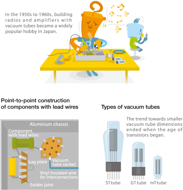
Tokyo's Akihabara district, home to the world-famous "Electric Town," is a Mecca for buying any kind of electronic component. As the saying goes," if you can't find it here, it doesn't exist." Akihabara has its roots in a cluster of small and medium-sized stores selling radio parts that sprang up around Akihabara station in the middle of the 20th century. At that time, building one's own radio from kit parts had become a popular hobby. As this was still the age of vacuum tubes, the radio builder would drill holes in an aluminum chassis, install vacuum tube sockets, transformers and other parts, and then connect the lead wires of resistors, capacitors etc. using a soldering iron. This method was known as "point-to-point construction."
In the 1960s, as transistors started to take over, the printed circuit board came into wider use and the point-to-point method eventually became obsolete. A printed circuit board (PCB) consists of an insulating resin base with a layer of copper foil on top. Unnecessary parts of the copper layer are removed by dissolving them in an etching process, thereby creating the desired circuit pattern. As the etching procedure was difficult to perform for the electronics hobbyist, universal boards with a large number of predrilled holes arranged in a grid pattern became popular. The leads of electronic components were pushed through the holes and then soldered on the reverse side of the board.
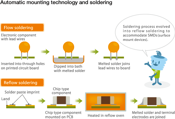
Initially, the manufacturing lines for electronic products all used manual labor, but to facilitate mass production, so-called inserters—machines for automatically mounting components in holes in printed circuit boards—were adopted. This process is known as "through hole" mounting. At the same time, the soldering step also was automated. After inserting the components with their leads in the printed circuit board, connections were established by dipping the assembly into a bath with molten solder. This is called flow soldering.
When chip components appeared in the 1980s, through hole mounting gradually gave way to another method that eventually became dominant, namely surface mounting by chip mounters. A component designed specifically for use with surface mounting technology (SMT) is called SMD (Surface Mount Device). As electronic components increasingly became SMD types, the soldering method also underwent a change. For surface mounting, solder paste is imprinted on the board on which the SMD components are placed. The entire assembly is then subjected to controlled heat by infrared radiation or hot air, thereby melting the solder and permanently connecting the joints. This process is called reflow soldering.
Miniaturization of chip components triggers advances in automated mounting techniques
Making electronic devices such as mobile phones and smartphones ever smaller was made possible by the amazing miniaturization of multilayer ceramic chip capacitors and other chip type components, which went hand in hand with advances in mounting technology. The 2012 size (2.0 x 1.2 mm) for chip components that dominated in the 1990s was replaced by the 1005 size (1.0 x 0.5 mm) in the first decade of the new millennium. Currently, even smaller sizes such as 0603 (0.6 x 0.3 mm) and 0402 (0.4 x 0.2 mm) have become common.
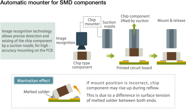
Mounting such tiny components on their correct locations on a printed circuit board by hand is all but impossible. As the use of tweezers or other mechanical means also involves the risk of damage, the chip components are mounted on the PCB using a suction nozzle. The principle here is the same as when sucking air through a straw to lift an object such as a piece of paper.
Positioning of the component on the printed circuit board of course requires high precision. Even a slight shift in position may cause the chip component to stick up when the solder paste is melted in the reflow oven. This phenomenon is called the Manhattan effect (also known as tombstoning), because the vertical chip then resembles the shape of a skyscraper. The effect is caused by a difference in surface tension of the melted solder at the left and right terminal electrodes of the component. High-accuracy image recognition technology is used to avoid such problems and achieve proper positioning.
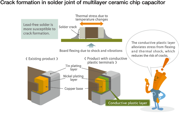
But even after successfully mounting the components on the circuit board, problems can still occur. Due to environmental considerations, the use of lead-free solder (tin, silver, copper alloys, or similar) has become the norm in recent years. Compared to conventional lead-based solder, lead-free solder is more susceptible to thermal expansion and contraction, and it also is harder and more brittle. If the printed circuit board is subject to flexing or shocks, cracks may develop in the solder joints. To solve this problem, TDK has introduced a new type of multilayer ceramic chip capacitor featuring a conductive plastic layer inserted between the copper base and the nickel plating of the external terminal electrode. The conductive plastic serves as a buffer that absorbs and alleviates stress from flexing or shocks, thereby significantly reducing the risk of cracks. This type of capacitor is especially suitable for use in the automotive environment, where temperatures range from extreme cold to searing heat, and vibrations and shocks are commonplace.
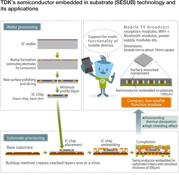
Semiconductor embedded in substrate (SESEB) technology
The circuit boards of mobile phones and smartphones are literally packed to capacity, taking high-density mounting of electronic components to the limit. Just as buildings in a crowded city center have no way to go but up, multilayer boards are used in such electronic devices to save space. This involves stacking of multiple circuit boards, with electrical connections between layers established by means of through holes.
While the miniaturization of passive components such as capacitors, inductors, and resistors into chip elements has been highly successful, integrated circuits still take up a considerable portion of the board surface. Even if the bare circuits (called bare chips or bare dies) left after cutting the wafer are small, the wire bonding required to connect a high number of leads results in considerable use of space. In recent years, progress has been made in this area by moving to flip-chip mounting, a technology where tiny protruding electrodes (called bumps) are created on the chip surface. The chip is then flipped over and mounted directly to the circuit board.
Semiconductor embedded in substrate (SESUB) technology takes this approach a decisive step further. Here the integrated circuit is not placed on the circuit board but rather embedded into the board itself. Likened to a densely populated metropolitan area, this would be similar to making effective use even of the layer of space beneath the surface of roads. However, even when embedded the thickness of the IC chip itself would still include a wasted component. TDK therefore has developed technology for polishing the rear side of the chip to a thickness of a mere 50 micron. By embedding such chips in a four-layer substrate, an IC embedded substrate with a total height of only 300 micron could be created. TDK calls this proprietary technology SESUB which stands for "Semiconductor Embedded in SUBstrate." The technology is not limited to embedding IC chips. It can also be applied to the creation of function modules that combine a number of electronic components. For example, TDK has used SESUB technology to develop highly compact, low-profile mobile TV broadcast reception modules, as well power supply modules for smartphones that require less than half the mounting area of existing modules.
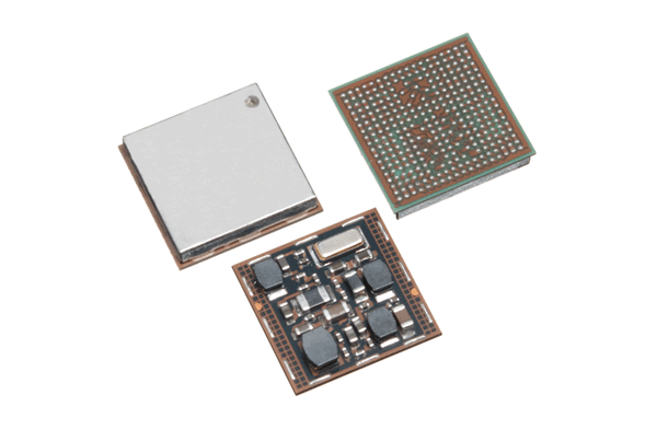
Power supply module realized with SESUB technology
Semiconductor embedded in substrate (SESUB) technology is still evolving and is expected to allow further miniaturization of electronic devices through the integration of circuit boards with electronic components.
TDK is a comprehensive electronic components manufacturer leading the world in magnetic technology
About TDK
Share Share this article
RecommendedPeople who viewed this article also viewed here
The Wonders of Electromagnetism
vol.5 Power Inductors in Mobile Phones
The Wonders of Electromagnetism
Discover the Workings of Highly Efficient Nuclear Batteries Used On Earth and In Space

Bridging the Past, Present, and Future of Tech
Smart Homes Revolution: How IoT is Making Homes Smarter and Safer
PickUp Contents