
Ferrite World
Vol. 11 Radio wave absorbers, anechoic chambers, and ferrite

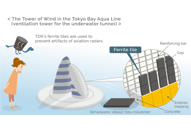
TDK’s ferrite tiles installed in the Tower of Wind in the Tokyo Bay Aqua Line
About two thirds of the Tokyo Bay Aqua Line, which connects Kawasaki City in Kanagawa Pref. and Kisarazu City in Chiba Pref., runs through an underwater tunnel. The Tower of Wind, which can be seen from far away like a huge yacht about 5km off the coast of Kawasaki, is a ventilation tower constructed to send air to and from this underwater tunnel.
Since the Tower is located near Haneda Airport, it is fitted with TDK’s ferrite tiles as radio wave absorbers. When radio waves from an aviation radar are reflected on a building, a non-existent object may appear as a radar image. This is called a radar artifact. A ferrite tile efficiently absorbs radio waves from radars and eliminates them as heat to prevent a radar artifact from occurring.
When television radio waves are reflected on a high-rise building, etc., a ghost occurs in the same way as a radar artifact. In order to prevent this, skyscrapers are also fitted with ferrite tiles. They are also used in platforms, etc. for Shinkansen bullet trains in order to prevent wireless communication failure in trains.
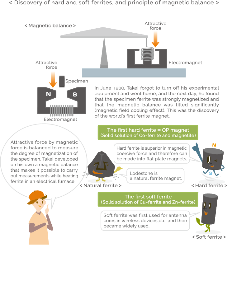
The first radio wave absorbers were put into practical use in the 1940s using non-magnetic materials such as carbon and graphite. The absorbers used these substances’ properties that some energy is converted into heat when radio waves pass through them due to the electrical resistance (ohmic loss) or dielectric loss of the materials. The principle was simple, but a considerable thickness was required in order to obtain sufficient absorption properties.
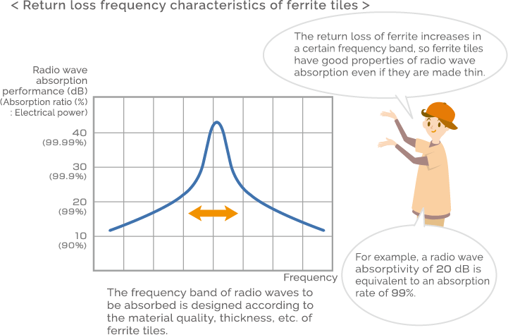
In the beginning of the 1960s, research made progress on how to use the unique magnetic properties of ferrite as a radio wave absorber. As seen in transformer cores, ferrite repeats magnetization reversal, following AC magnetic fields smoothly. However, when frequencies increase to a MHz or higher band, even ferrite finally becomes unable to follow changes in magnetic fields, and the magnetic permeability drops in a certain frequency band, resulting in sharp increases in magnetic loss (state called natural resonance). While the use of ferrite in transformer cores, etc. is avoided in such a frequency band, this characteristic is proactively used in ferrite radio wave absorbers. Their great advantage is that they can be made extremely thin, as compared with other radio wave absorbers (a thickness of ferrite tiles is about 6mm). Also, ferrite tiles are a sintered ceramic, so they are compatible with concrete, exterior porcelain tiles, etc. and are suitable as radio wave absorbers for outdoor buildings.
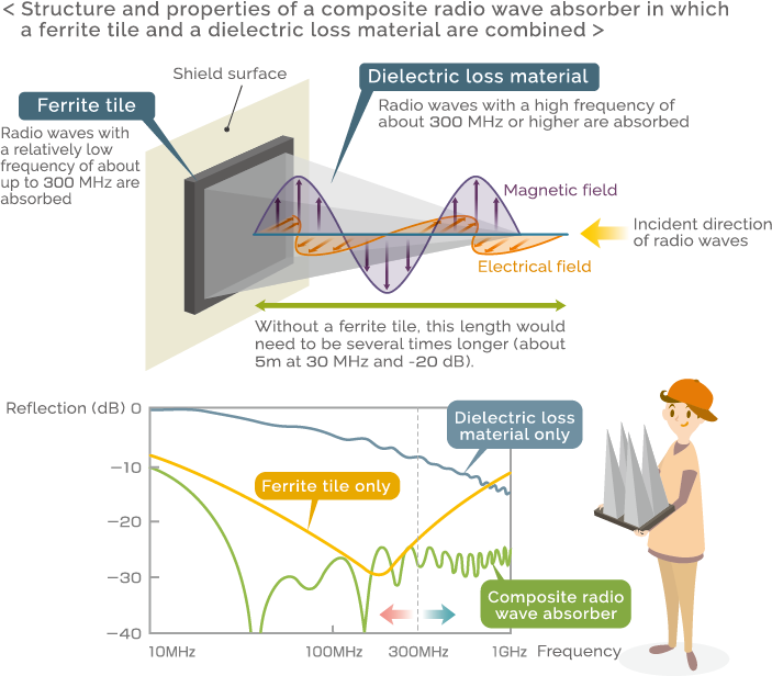
Composite radio wave absorbers in which a ferrite tile and a dielectric loss material are combined
The masts of ships and vessels are fitted with radio wave absorbers in which ferrite powder is mixed with rubber, etc. This is because if radio waves emitted from a vessel’s radar are reflected on a mast of the vessel, a radar artifact appears. This is similar to the “self-poisoning problem” in mobile phones, etc. It is a noise failure that electromagnetic noise generated in a circuit gives a functional damage back to the circuit itself. In mobile phones, in order to address this self-poisoning problem, a magnetic shield material (TDK’s Flexield product) is attached on surfaces of ICs, etc. This material is made by mixing high-magnetic-permeability material powder with elastic resin, and acts as an electromagnetic noise absorber in electronic devices.
Radio wave absorbers are also materials necessary for anechoic chambers. Anechoic chambers are shielded spaces that are designed and constructed so that they are not affected by external electromagnetic waves and prevent internal electromagnetic waves from getting outside. Originally, they were facilities for experiment and research on wireless equipment, antennas, etc., and after the 1980s, they were widely constructed as an EMC measure for electronic devices because noise regulations for electronic devices started to be enforced on a full scale. The EMC measure is an attempt to implement both emission and immunity measures: the former is to suppress radiation noise that have external effects while the latter is to provide immunity against external radiation noise.
The measurement of the electrical field intensity of electromagnetic noise emitted from electronic devices is standardized as an outdoor open-site measurement. However, various radio waves come and go outside, and moreover weather conditions such as wind and rain adversely affect measurements. Also, during immunity tests, since extremely strong electrical fields are applied, outdoor open-site measurement is difficult to carry out due to the Radio Act, etc. This is why anechoic chambers are used. Anechoic chambers vary depending on the size or application of the device or system to be evaluated, and generally, 10m and 3m anechoic chambers are used in EMC tests for electronic devices.
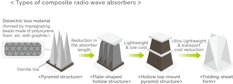
EMC tests for electronic devices extend over a very wide frequency bandwidth from the MHz to GHz bands, and ferrite alone cannot cover it. Thus, composite radio wave absorbers in which different radio wave absorbers are combined are used. Radio waves with a relatively low frequency of about 300 MHz or less are absorbed by using magnetic loss of a ferrite tile, and higher-frequency radio waves are absorbed by using dielectric loss materials with a pyramid, tapered or other structure. These composite radio wave absorbers were devised in Japan (through research by Dr. Kunihiro Suetake, Dr. Yoshiyuki Naito, and Dr. Yasutaka Shimizu at Tokyo Institute of Technology).
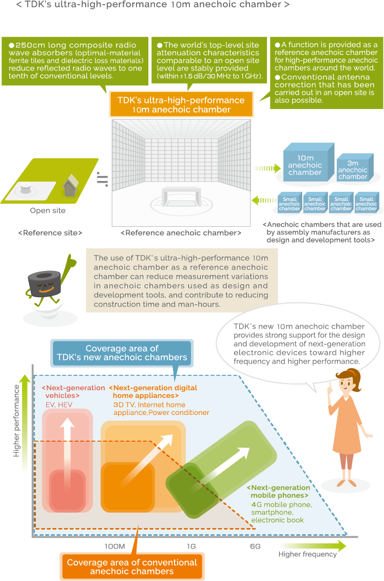
New evolution of anechoic chambers––the World’s top-level ultra-high-performance 10m anechoic chambers
In 1969, TDK constructed the world’s first anechoic chamber using ferrite radio wave absorbers. Since then, TDK has provided more than 1,000 anechoic chambers around the world (about 500 in Japan and 500 in foreign countries).
With increased digitization and higher functionality of electronic devices, EMC measures are being further stepped up, and small-sized anechoic chambers or 3m or 10m anechoic chambers are utilized in order to reduce construction time and man-hours. However, high traceability and reproducibility are important for EMC measurement in an anechoic chamber. The error margin between an ideal open site and an anechoic chamber (site attenuation characteristics) is stipulated as within ±4dB, but in reality, it needs to be from ±3dB to ±2dB, and has been made stricter to within ±2dB in recent years.
Manufacturing requires accurate scales, but even if there is some variation in scales, errors can be reduced to within an acceptable range by carrying out corrections with an accurate standard scale. Similarly, EMC testing requires an accurate standard anechoic chamber. This role is taken by a new anechoic chamber building that was constructed in TDK Technical Center (Ichikawa City, Chiba Pref.) and launched a full-scale operation in June 2010.
TDK’s new anechoic chamber building is the world’s top-level facility that includes 10m and 3m anechoic chambers for EMC tests, micro-wave and millimeter-wave anechoic chambers for antenna measurement, and a shielded room that can carry out simple measurement. The 10m anechoic chamber is an ultra-high-performance new anechoic chamber that has a site attenuation characteristics of ±1.5dB or less, and is used as a reference for anechoic chambers used around the world (a reference anechoic chamber).
In recent years, anechoic chambers have come to play significantly important roles as not only simple measurement and testing facilities, but also design and development tools for new products. TDK’s ultra-high-performance 10m anechoic chamber can address future revisions to EMC standards toward higher frequency and higher immunity. It provides total support for development of next-generation electronic devices, such as smartphones, electronic books, and 3D TVs, ranging from design and prototyping to evaluation and certification steps.
TDK is a comprehensive electronic components manufacturer leading the world in magnetic technology
Share Share this article
RecommendedPeople who viewed this article also viewed here
Ferrite World
Vol. 12 Evolution of ferrite magnets by combination of materials, molding, and sintering technologies

Ferrite World
Vol. 13 Ferrite is a material with unlimited potential

Bridging the Past, Present, and Future of Tech
Smart Homes Revolution: How IoT is Making Homes Smarter and Safer
PickUp Contents