
Ferrite World
Vol. 10 Layering/thin-film technologies and ferrite
The world’s first commercialized TDK multilayer chip inductors
A coil used as an electronic component in a mobile phone, personal computer, etc. is also referred to as an inductor. This is because such a coil produces an inductive electromotive force in response to changes in magnetic flux (electromagnetic induction phenomenon). The intensity of the force is called the inductance of the coil (the unit is H or henry), and increases in proportion to the section area of the coil, the square of the number of turns in the coil, and the magnetic permeability of the core.
Inductors for electronic components are roughly classified into coil inductors, multilayer inductors, and thin-film inductors, according to the manufacturing method. Typically, power inductors (inductors for power supplies), to which a high current is applied, are coil inductors. A coil power inductor has a structure in which a ferrite drum core is wound with copper wire and can offer high inductance, despite its small size, by using a ferrite core with high magnetic permeability and low loss. Also, such a ferrite core can reduce the number of turns of copper wire even at the same inductance, so it helps reduce the DC resistance (Rdc) of copper wire and also contributes to reduction in battery power consumption.
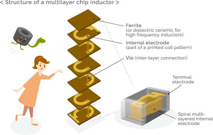
Multilayer chip inductors are mainly used in filter circuits, impedance matching circuits, etc. on signal lines. They are manufactured by layering many ferrite sheets on which a coil pattern is printed using pasty metal material (e.g., Ag). They became the world’s first commercialized inductors in 1980 by TDK and were first used as SMD (surface mount device) inductors for portable radios. Currently, they are widely used in various electronic devices. They have a structure in which a three-dimensional coil is completely covered with ferrite, so the magnetic shield effects of ferrite reduce magnetic leakage, making them suitable for high-density mounting on circuit boards.
The magnetic permeability of ferrite changes depending on the frequency. At high frequencies of several hundred megahertz or more, ferrite causes greater loss and becomes unable to be used. Thus, multilayer inductors using dielectric ceramic as the base material instead of ferrite are used as high-frequency ones.
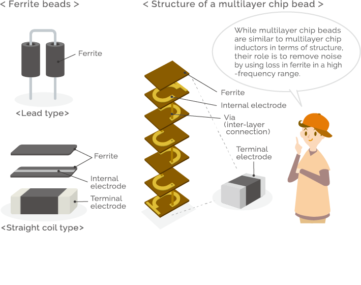
Loss in ferrite gradually increases at high frequencies. Ferrite beads use this characteristic of ferrite as an advantage. Multilayer chip beads are manufactured by forming a spiral conductive line pattern in ferrite using a layering method. While multilayer chip beads are similar to multilayer chip inductors in terms of structure and manufacturing method, they absorb high-frequency noise components as loss and filter them out as heat.
Thin-film common-mode filter to which thin-film technology for HDD heads is applied
In recent years, there has been a demand for smaller and also lower-profile multilayer chip components, due to the use of multilayer printed circuit boards and the progress of modularization by which electronic components are embedded in ceramic multilayer substrates (LTCC or low temperature co‐fired ceramics), etc. TDK has developed a thin-film process technology through the manufacture of HDD heads to establish a manufacturing technology for thin-film inductors in which a metal-conductor thin-film coil is formed on a ferrite substrate. TDK offers various thin-film devices such as thin-film common-mode filters and thin-film BPF (band pass filters).
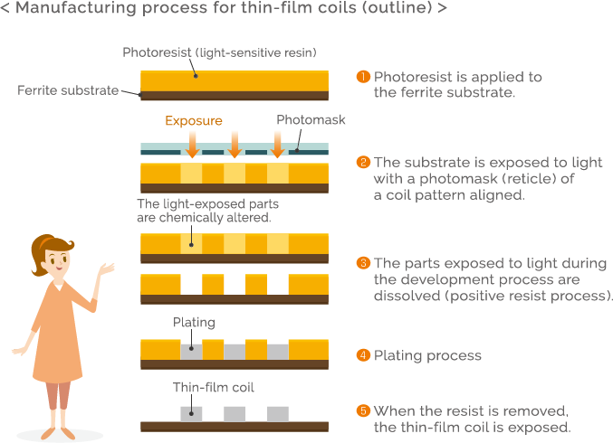
A thin-film inductor is manufactured by forming a spiral thin-film coil on a substrate through the repetition of processes such as photolithography and plating, in the same way as for the coil of the write device in an HDD head. Photoresist (light-sensitive resin) is applied to a substrate, and a coil pattern is developed through lithographic exposure and transcription, using a photo mask. As a result, the resist in the unexposed regions is deposited. (This is called a positive resist process, in which the exposed parts are dissolved. A process in which exposed parts remain insoluble is called a negative resist process.) The substrate is plated and the resist is removed. Then, the plate layer appears as the coil pattern.
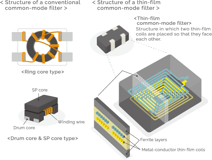
TDK’s thin-film common-mode filters have been developed using this thin-film inductor technology. As described in Vol.8 of this series, the basic structure of a common-mode filter is a ferrite ring core that is wound with two wires in the same direction. It is an EMC (electromagnetic compatibility) component that only removes common-mode noise without affecting signal currents. In order to provide compatibility with automatic winding, a small SMD common-mode filter has a structure in which a drum core, instead of a ring core, is wound with a conductive wire and is fitted with a flat-plate SP core so that the entire cores are made into a ring configuration. While TDK has commercialized 2012-size (2.0 × 1.2 mm) components that are smaller than rice grains, there has been a demand for even smaller and lower-profile components for mobile phones, etc., in which the space-saving of circuits has been pursued to the utmost.
In response to such market needs, TDK has developed a thin-film common-mode filter. It has a multilayer structure in which two thin-film conductor coils are placed in a ferrite layer so that they face each other. A significant space saving has been achieved thanks to this thin-film common-mode filter, reducing mounting areas to less than half a typical size.
Thin-film common-mode filter in which an ESD protection device is embedded by a thin-film method
Cables passing high-speed digital signals, such as USB cables and HDMI cables, function as an antenna that emits noise, so they need to incorporate a common-mode filter in their interfaces as an EMC measure. Meanwhile, mobile devices such as mobile phones, smartphones, digital cameras, and portable music players are often touched by hands, so they need ESD (electrostatic discharge) measures for their interface terminals separately from measures against common-mode noise. This is because electrostatic discharge from a human body amounts to several thousand volts and may cause problems such as malfunction of circuits and destruction of ICs if no measures are taken.
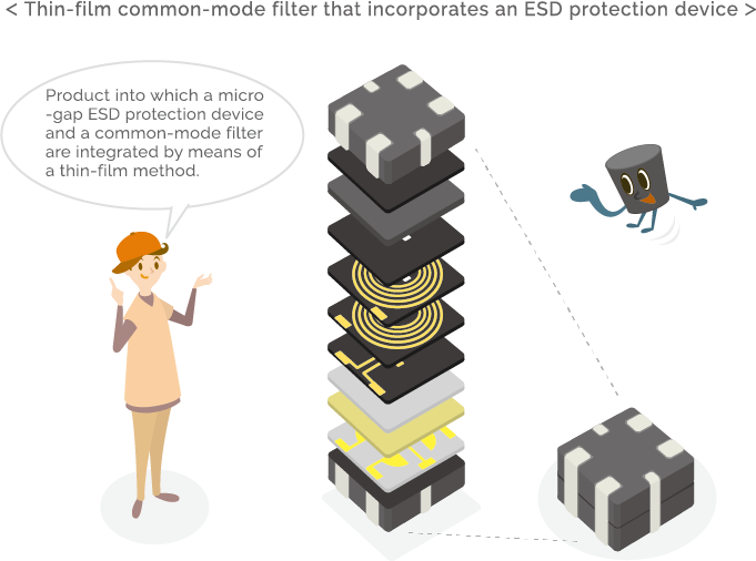
Thus, TDK has newly developed a common-mode filter that incorporates an ESD protective device. Semiconductor-ceramic varistors are used as ESD protection components. However, the inter-terminal capacitance of varistors (the capacitor component between terminals) is becoming unable to meet the required properties as high-speed digital interfaces advance.
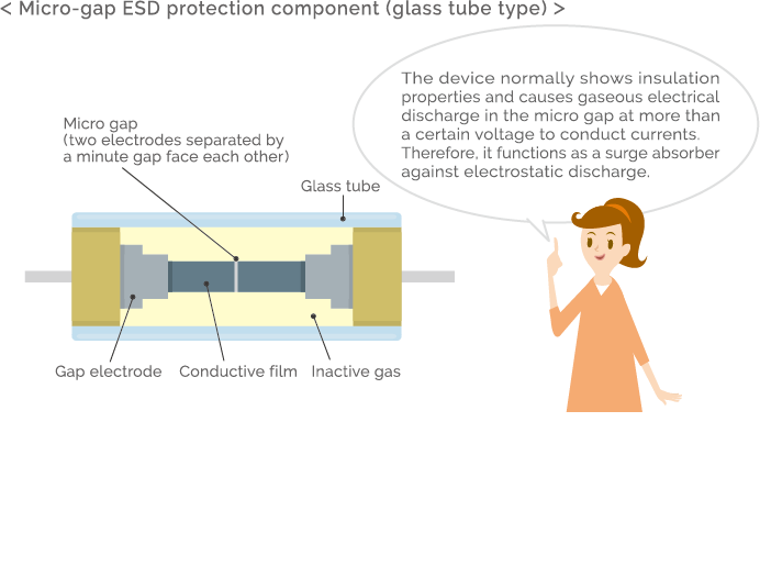
Therefore, attentions are focused on a micro-gap ESD protection component with a small inter-terminal capacitance. This is a device in which two electrodes are placed so that they face each other with a minute gap between them. When static electricity from a human body is applied, electrical discharge occurs in the gap to protect the circuit. Conventionally, devices such as those in which electrodes are enclosed in a glass tube have been used. Meanwhile, TDK has established a technology to form a micro-gap ESD protection device as a thin film on the multilayer structure of a thin-film common mode filter, by applying an advanced thin-film process technology. A highly advanced technology is needed to form a micro-gap ESD protection device by means of a thin-film method. TDK has resolved this issue by, for example, selecting optimal material and devising a gap electrode structure that can offer stable properties. The integration of two functional devices by means of a thin-film method reduces the number of components and mounting areas, and greatly contributes to miniaturization and high functionality of mobile devices.
TDK is a comprehensive electronic components manufacturer leading the world in magnetic technology
Share Share this article
RecommendedPeople who viewed this article also viewed here
Ferrite World
Vol. 11 Radio wave absorbers, anechoic chambers, and ferrite
Ferrite World
Vol. 12 Evolution of ferrite magnets by combination of materials, molding, and sintering technologies

Bridging the Past, Present, and Future of Tech
Smart Homes Revolution: How IoT is Making Homes Smarter and Safer
PickUp Contents