
Understanding the Types and Roles of Capacitors through Five Articles | The World of Power Capacitors
Part 5: The Technological Innovations in Multilayer Ceramic Chip Capacitors

- A thousand times more capacitance in the same shape—and a hundred times smaller with the same capacitance

- How multilayer ceramic chip capacitors are manufactured
- A variety of core technologies are required—including materials, lamination, and sintering
- TDK was the first to commercialize production technologies for nickel-based internal electrodes
- ULI for low-voltage ICs and LSIs, and next-generation ULI
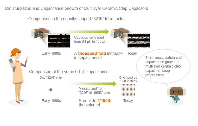
A thousand times more capacitance in the same shape—and a hundred times smaller with the same capacitance
In the world of semiconductors, there is a proverbial saying known as Moore’s Law, which predicts that the number of transistors on a silicon microchip will double every two years. Another electronic component has achieved miniaturization at a similarly dramatic pace: the multilayer ceramic chip capacitor.
As many as 300 multilayer ceramic chip capacitors are used in a typical mobile phone, and more than a thousand in a PC or game console. It is fair to say that the downsizing and weight reduction of mobile devices and other electronic products would have been impossible without the miniaturization of multilayer ceramic chip capacitors.
The primary benefit of multilayer ceramic chip capacitors is their ability to provide high capacitance in small dimensions, achieved by stacking a large number of electrodes. In the early 1980s, a chip capacitor in the “3216” form factor (3.2 by 1.6 mm) had a capacitance of 0.1 µF, but that figure has reached 100 µF today—a thousand-fold increase. This matches electrolytic capacitors, which are characterized by high capacitance. A comparison at the same capacitance shows that miniaturization has also progressed considerably. For example, a 0.1 µF capacitor that was in the “3216” size in the early 1980s has now been reduced to the “0603” size—just 0.6 x 0.3 mm. This translates to approximately one-hundredth the volume. This is smaller than a strawberry seed—so small that it is difficult to discern with the naked eye.
How multilayer ceramic chip capacitors are manufactured
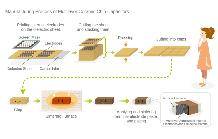
The use of multilayer ceramic chip capacitors in consumer electronic devices began with pocket radios in the 1970s. Originally, they were developed for use in spacecraft—where small size and durability were paramount—and their manufacturing process is very different from other types of capacitors.
First, refined raw material powder is formed into a paste, cast thinly across a carrier film, then dried to produce a dielectric sheet called a “green” (meaning raw) sheet. This sheet is screened-printed with a metallic paste that forms the internal electrodes. Dozens, hundreds, or more than a thousand of these sheets are stacked together, pressed, cut into chip size, and sintered in a furnace—creating hardened, ceramic chips. Finally, paste material that forms the external electrodes is applied on both ends, sintered and plated—and a multilayer ceramic chip capacitor is born.
A variety of core technologies are required—including materials, lamination, and sintering
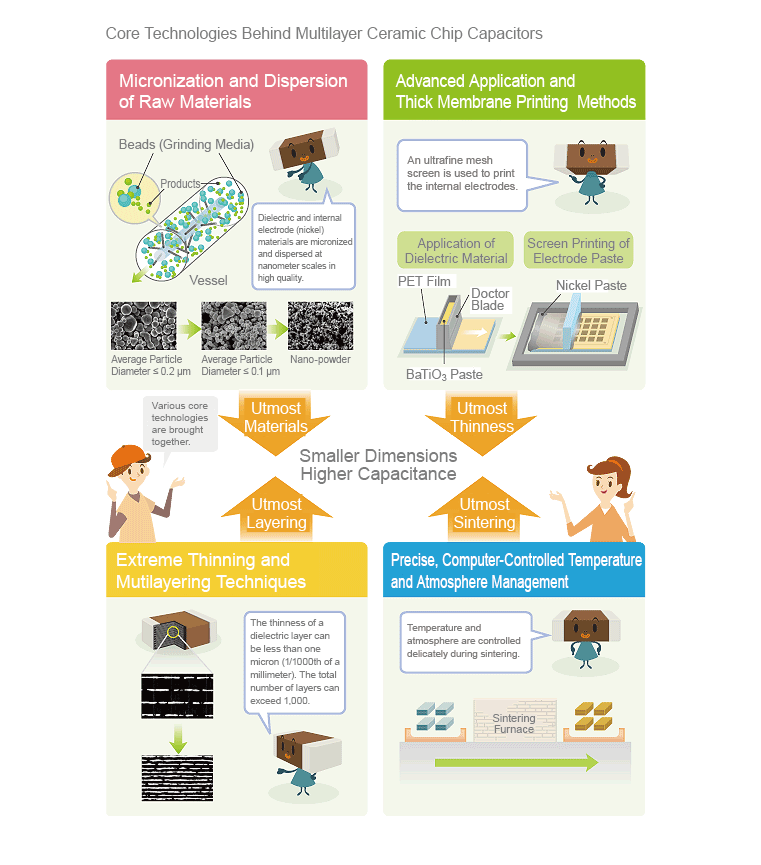
Multilayer ceramic chip capacitors are manufactured by integrating a variety of core technologies. Techniques for making the dielectric and internal electrode sheets thinner are especially key to miniaturization and achieving higher capacitance. In chips where the number of layers reaches a thousand, the thinness of each dielectric sheet can be less than one micron (µm). This is less than one-hundredth the thickness of a regular piece of paper and less than one-tenth the thickness of plastic food wrap. Consequently, multilayer ceramic chip capacitors require advanced nanotechnologies. TDK has achieved the utmost in thinness by embracing technologies to micronize and disperse dielectric and nickel particles that form the internal electrodes at nanometer scales.
Dielectric sheets are thin, brittle, and easily fractured. Stacking them with high precision without misalignment or delamination from the carrier film requires cutting-edge technologies. The gaseous environment inside the furnace during sintering is referred to as the atmosphere, and precise control of the atmosphere and temperature is critical.
TDK was the first to commercialize production technologies for nickel-based internal electrodes
Multilayer ceramic chip capacitors are sintered at temperatures ranging from around 1,000 to 1,300°C. Sintering in an ordinary atmosphere results in oxidation of the internal electrodes; yet, sintering in a reductive atmosphere with little oxygen reduces the dielectric into a semiconductor, deteriorating the capacitor’s characteristics. This is why precious metals that do not oxidize readily—such as palladium and silver—were used for internal electrodes in the past. With the rapid growth of electronics, however, the consumption of capacitors soared, creating demand for new technologies that would allow internal electrodes to be produced using inexpensive base metals. Responding to this demand, TDK became the first to develop and successfully commercialize the technologies required to mass-produce nickel-based internal electrodes for multilayer ceramic chip capacitors.
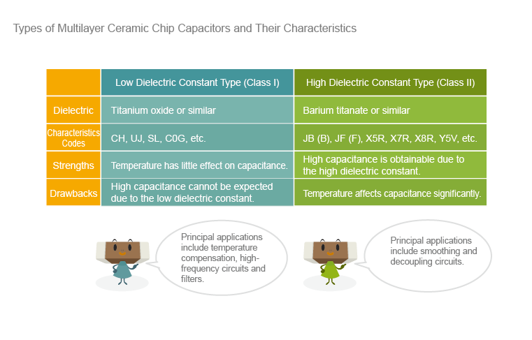
There are two types of multilayer ceramic chip capacitors: low (Class I) and high (Class II) dielectric constant types, differentiated by their temperature characteristics. TDK achieved the production of nickel internal electrodes in the high dielectric constant types in 1988, followed by the low dielectric constant types in 1999—which had been considered nearly impossible.
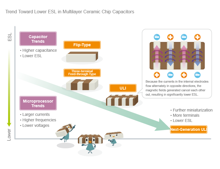
ULI for low-voltage ICs and LSIs, and next-generation ULI
TDK is a comprehensive electronic components manufacturer leading the world in magnetic technology
Share Share this article
RecommendedPeople who viewed this article also viewed here

Sports Tech@TDK
How do Breaking balls work? Why Do Breaking Balls Curve? Curves, Shoot, and Sliders...

Sports Tech@TDK
Making the World Cup More and More Exciting with the VAR System and Football Sensor Technology - Offsides determined by VAR-

Bridging the Past, Present, and Future of Tech
Smart Homes Revolution: How IoT is Making Homes Smarter and Safer
PickUp Contents